
Why Thin-Film Lithium Niobate Is Emerging as a Key Platform for High-Speed Optical Modulators
2026-09-22
The explosive growth of artificial intelligence, high-performance computing, and cloud data centers is driving unprecedented demand for higher-bandwidth, lower-power optical communication systems. As networks progress from 400G to 800G, 1.6T and beyond, optical modulators face increasingly stringent requirements in bandwidth, drive voltage, signal integrity, size, and integration density.
As the core component of an optical transmitter, the modulator converts high-speed electrical signals into modulated optical signals. Its performance directly determines the capacity and efficiency of the entire optical link. Against this backdrop, thin-film lithium niobate (TFLN) has rapidly emerged as one of the most promising technology platforms for next-generation high-speed modulators. By combining the exceptional electro-optic properties of bulk lithium niobate with thin-film waveguide architectures, TFLN enables higher modulation speeds, lower drive voltages, smaller footprints, and greater potential for photonic integration.
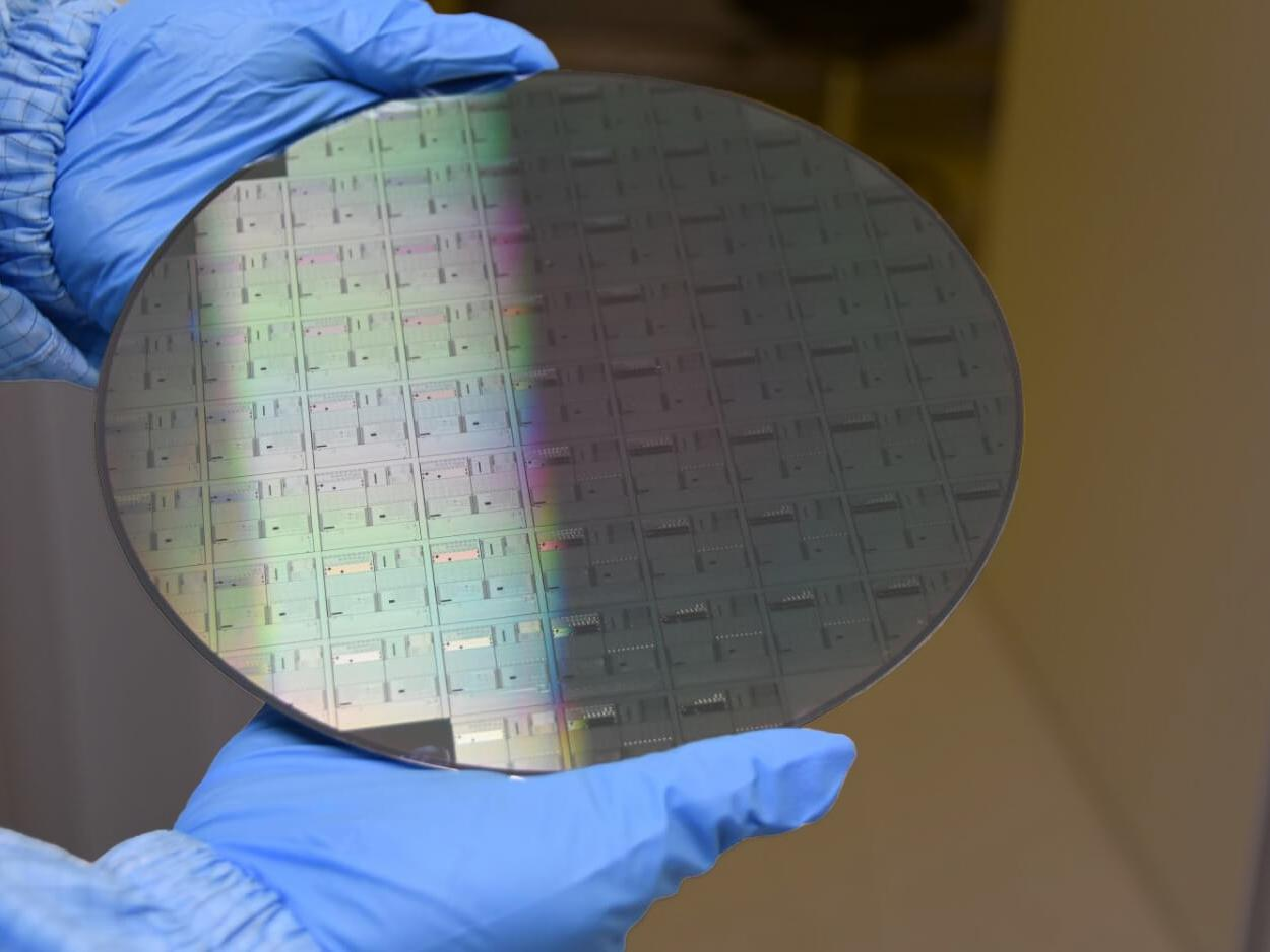
1. Why Lithium Niobate Remains Essential for Optical Modulation
Lithium niobate (LiNbO₃) has long been a cornerstone material in electro-optic modulation, nonlinear optics, and optical signal processing. Its strong Pockels effect allows an applied electric field to change the refractive index linearly and at extremely high speed, enabling pure phase or intensity modulation without free-carrier effects.
Conventional bulk lithium niobate modulators have served optical communications reliably for decades. However, their relatively large size, high drive voltages, and limited integration density no longer meet the demands of modern high-speed, high-density optical modules. Thin-film lithium niobate addresses these limitations by transferring a sub-micron lithium niobate layer onto a low-index substrate (typically silicon or quartz) and patterning high-confinement optical waveguides and coplanar electrodes. The resulting platform retains the superior electro-optic coefficient of lithium niobate while offering dramatically improved optical confinement, electrode–optical mode overlap, and device compactness.
2. Key Advantages of TFLN Modulators
High-speed electro-optic response
Lithium niobate’s intrinsic electro-optic bandwidth is extremely high. When combined with carefully engineered travelling-wave electrodes, velocity matching, and low-loss microwave design, TFLN modulators routinely demonstrate electro-optic bandwidths exceeding 100 GHz, making them strong candidates for 800G, 1.6T and future higher-baud-rate systems.
High modulation efficiency
The tight optical confinement of thin-film waveguides significantly increases the overlap between the optical mode and the applied RF field. This improves the voltage–length product (Vπ·L), allowing shorter devices or lower drive voltages—both critical for reducing power consumption and enabling denser integration.
Wideband operation
Proper electrode design, impedance matching, and packaging enable TFLN modulators to support the multi-lane, high-baud-rate electrical interfaces required by next-generation coherent and intensity-modulation direct-detection (IM-DD) systems.
Lower power consumption potential
Improved modulation efficiency and shorter interaction lengths can reduce the required RF drive power. When combined with advanced driver electronics and packaging, TFLN-based transmitters offer a clear path toward lower overall system power.
Miniaturization and photonic integration
TFLN supports compact, low-loss waveguides and is compatible with hybrid or heterogeneous integration of lasers, detectors, and electronic drivers. This opens the door to denser optical engines and more sophisticated photonic integrated circuits.
3. TFLN in the Evolution Toward 800G, 1.6T and Beyond
Optical interconnects are evolving rapidly to support the traffic generated by AI clusters and hyperscale data centers. Achieving 800G and 1.6T modules requires simultaneous advances in lasers, modulators, drivers, packaging, and digital signal processing.
TFLN is particularly well suited to this transition because it combines:
· High electro-optic bandwidth
· Low drive voltage
· Compact footprint
· Potential for multi-channel and multi-function integration
Its ultimate suitability for any specific module architecture still depends on the chosen modulation format (PAM4, coherent, etc.), symbol rate, packaging approach, and system-level power and thermal constraints. Nevertheless, the platform has already demonstrated performance levels that place it among the leading candidates for next-generation optical engines.
4. Beyond Discrete Modulators: Toward Photonic Integration
TFLN is more than a modulator material. The same thin-film platform supports a wide range of photonic functions, including:
· High-speed phase and intensity modulators
· Optical frequency combs and nonlinear frequency conversion
· Microwave photonic filters and true-time-delay lines
· Optical switches and signal processors
Hybrid integration with silicon photonics, III–V lasers, or CMOS electronics further expands its application space, helping bridge the gap between discrete components and highly integrated photonic systems.
5. Remaining Engineering Challenges
Despite its strong technical potential, widespread commercial adoption of TFLN still requires progress in several areas:
· Fabrication consistency — Sidewall roughness, film uniformity, and process control directly affect optical loss and yield.
· High-frequency packaging — RF performance measured on-chip must be preserved after packaging and assembly with drivers.
· Heterogeneous integration — Seamless co-packaging or hybrid bonding with lasers, drivers, and control electronics remains non-trivial.
· Manufacturing scalability — Transitioning from research wafers to high-volume production demands robust process control, testing infrastructure, and supply-chain maturity.
Addressing these challenges is essential for TFLN to move from promising laboratory results to reliable, cost-effective commercial modules.
6. Outlook
Driven by the relentless bandwidth demands of AI infrastructure and data-center interconnects, thin-film lithium niobate has established itself as a key enabling technology for high-speed optical modulation. Its unique combination of high electro-optic coefficient, tight optical confinement, and integration potential positions it strongly for 800G, 1.6T and future optical systems. Beyond conventional communications, TFLN is also finding applications in optical computing, microwave photonics, LiDAR, sensing, and quantum photonics. The pace of commercial adoption will ultimately be determined by continued improvements in device performance, packaging, yield, and system-level cost.
Conclusion
Thin-film lithium niobate represents a significant advance in electro-optic modulator technology. By marrying the proven material advantages of lithium niobate with modern thin-film waveguide and electrode engineering, TFLN delivers the bandwidth, efficiency, and integration density required by next-generation optical networks. As the industry moves from 400G toward 800G, 1.6T and beyond, continuous innovation across materials, device design, packaging, and system integration will be critical. TFLN stands out as one of the most promising platforms to meet these challenges and shape the future of high-speed optical communication.
GLSUN remains committed to advancing optical technologies across the full stack—from chips and devices to modules and systems—helping customers realize the performance and integration benefits that thin-film lithium niobate enables.