
Four Major Technology Routes for OCS Optical Circuit Switches
2026-03-24
In the era of artificial intelligence (AI) large model training, data center computing clusters are growing exponentially, from thousands of chips in Google's TPU systems to millions of cards in NVIDIA's GB200 clusters. This places unprecedented demands on network interconnects for bandwidth, latency, and power consumption. Traditional electrical packet switches (EPS) rely on optical-electrical-optical (OEO) conversions, which result in high power consumption (tens of watts per port), significant latency (microsecond level), and frequent port rate upgrades. Optical Circuit Switches (OCS) have emerged as a solution. By enabling pure optical path reconfiguration, OCS completely eliminates OEO stages, achieving "zero-power switching," sub-millisecond reconfiguration, and rate-agnostic operation (seamless support for 400G/800G/1.6T upgrades).
The core of OCS is the optical switching matrix, which establishes physical light paths between any input and output ports, much like an "automated railway marshalling yard": trains (optical signals) travel directly along dedicated tracks without needing to open the carriages for inspection. Compared to the "postal sorting" model of EPS, OCS can reduce data center energy consumption by 30%-50%, shorten network reconfiguration time to the millisecond level, and support ultra-large-scale expansion. It has become a core technology choice for hyperscalers such as Google, NVIDIA, and Microsoft. In the three major AI scenarios—Scale-Up (within a single cluster), Scale-Out (across racks), and Scale-Across (across data centers)—OCS is gradually replacing the Spine layer of electrical switches and becoming the "nervous system" of AI computing networks.
Currently, OCS technology routes have not fully converged. Globally, four major mainstream routes have formed: MEMS (Micro-Electro-Mechanical Systems), Digital Liquid Crystal (DLC/LCoS), Direct Light Beam Steering (DLBS/CLBS, also known as piezoelectric ceramic), and Silicon Photonics (Si Photonics). Each has its strengths and weaknesses. MEMS currently dominates the market (with over 70% share), while the other routes excel in reliability, insertion loss, speed, and cost. As AI computing power evolves toward 1.6T+, the four routes will evolve in parallel, with potential long-term convergence toward silicon photonic integrated solutions. The following sections analyze them one by one.
MEMS Technology: Current Mainstream and Mature Commercial Choice
MEMS (Micro-Electro-Mechanical Systems) is the highest-market-share technology route, accounting for over 70%. Its core consists of an input/output fiber collimator array (FAU) and a MEMS micromirror array forming an N×N optical switching matrix. The working principle involves electrically controlling the two-dimensional tilt angles (X/Y axes) of hundreds-of-microns-scale micromirrors to reflect input light beams precisely to the target output ports. The micromirrors are fabricated using semiconductor processes, primarily driven by electrostatic comb actuators, with precise alignment achieved by adjusting bias voltages for sub-millisecond response.
Typical Structural Diagram (MEMS micromirror array reflecting optical paths):
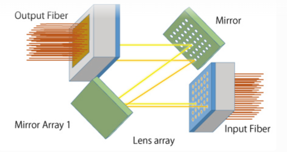
MEMS offers low insertion loss (typically <3 dB), strong port scalability (hundreds of ports already commercialized), high reliability (Lumentum MEMS micromirrors have accumulated over 1 trillion hours of failure-free operation), and balanced cost-performance. Google extensively uses MEMS OCS in its TPU v4/v5/Ironwood clusters. In the Jupiter architecture, 48 units of 136-port OCS build 3D Torus topologies for 4096–9216 TPUs, completely replacing the Spine layer of electrical switches and enabling optical path reconfiguration.
Disadvantages: Switching time is approximately 25 ms (due to mechanical motion), with long-term challenges in port count limits (mechanical fatigue) and alignment precision during large-scale expansion.
Digital Liquid Crystal (DLC/LCoS) Technology: Highest Reliability with No Moving Parts
Digital Liquid Crystal (DLC) or Liquid Crystal on Silicon (LCoS) technology originates from mature Wavelength Selective Switch (WSS) processes and uses an all-solid-state design with no mechanical moving parts. The principle involves applying an electric field to change the arrangement of liquid crystal molecules, affecting the polarization state of incident light. Input light is split into S and P polarization components, processed separately, and recombined at the output to achieve path switching. Coherent and other vendors offer both DLC and LCoS solutions.
Working Principle Diagram (DLC panels and beam collimation):
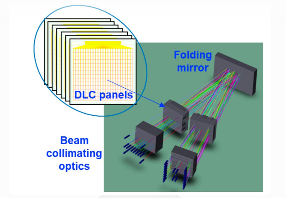
Advantages: World-leading reliability (no moving parts; claimed lifetime 10× that of MEMS), lower cost (around $40,000 per unit), and extremely high stability—ideal for large-scale Spine layer applications that do not require frequent reconfiguration. Switching speed is approximately 100 ms, but power consumption is extremely low.
Disadvantages: Slower switching, unsuitable for high-frequency reconfiguration scenarios.
This route excels in high-stability scenarios (e.g., financial data centers or ultra-large-scale AI training) and has been validated in global deployments.
Direct Light Beam Steering (DLBS/CLBS, Piezoelectric Ceramic) Technology: Lowest Loss with Strong Long-Term Potential
Also known as piezoelectric or Direct Light Beam Steering (DLBS), this approach leverages the axial dimensional change of piezoelectric ceramics under voltage to directly drive fiber collimators for spatial displacement and angular deflection. Core components include fiber collimators, two-dimensional piezoelectric actuators, and precise position sensors. Two collimator arrays face each other, achieving precise port alignment through electromechanical coupling.
Advantages: Simplest optical path, lowest transmission loss (minimal insertion and return loss), no traditional mechanical mirror fatigue issues, and greater physical scalability. Faster switching and strong expansion potential, especially suited for high-performance, low-loss scenarios.
Disadvantages: As port counts increase, the mechanical displacement required for large-angle alignment limits scalability, and costs are higher; currently more used in performance benchmarking.
Silicon Photonics (Si Photonics) Technology: Fastest Switching and the Ultimate Future Solution
This route integrates predefined optical path matrices on silicon chips, with light signals propagating along waveguides and switching achieved via thermo-optic/electro-optic effects or Semiconductor Optical Amplifiers (SOA). Theoretical switching speeds reach microseconds or even nanoseconds, leveraging mature CMOS processes for high-density integration.
Typical Silicon Photonic Integration Diagram (chip-level optical paths with SOA compensation):
Advantages: Fastest switching (<100 μs), greatest potential for cost reduction (compatible with mature CMOS foundries), easy high-density integration, and loss compensation via SOA. Completely rate-agnostic, ideal for future 1.6T+ ultra-large-scale clusters.
Disadvantages: Currently higher loss, unresolved multi-channel crosstalk, and reliability issues; not yet in large-scale commercial use.
The industry generally considers silicon photonics the "ultimate solution," especially as AI computing scales to millions of cards, where its integration density and cost advantages will become prominent.
Comparison of the Four Technology Routes
Switching Time: MEMS ~25 ms; DLC ~100 ms; DLBS faster; Si Photonics <100 μs (fastest).
Insertion Loss: DLBS lowest; MEMS/DLC low; Si Photonics higher (compensable).
Reliability: DLC highest (no moving parts); MEMS high; DLBS/Si Photonics high potential.
Port Scalability: MEMS strongest; Si Photonics strong CMOS potential; DLBS limited by mechanical displacement.
Cost: DLC lower; MEMS balanced; DLBS higher; Si Photonics lowest in the future.
Applicable Scenarios: MEMS (current large-scale commercialization); DLC (high-reliability Spine); DLBS (low-loss high-end); Si Photonics (future integrated endgame).
The four routes complement each other; no single route has absolute dominance, and they are in a phase of "co-evolution."
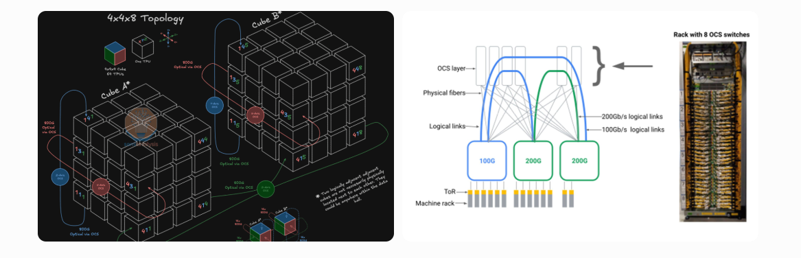
Example of Google AI Data Center OCS Deployment (TPU topology and rack photos):
Current Market Status and Industry Chain Layout
The global OCS market is accelerating explosively. Google has mass-produced its sixth-generation TPU v6 and is deploying MEMS OCS at scale; NVIDIA's DCI (Data Center Interconnect), Microsoft, Meta, and others are following. After 2025, Direct Light Beam Steering and silicon photonic solutions are expected to become dominant. Market size is projected to grow rapidly from the current hundreds of millions of dollars to over $1.6 billion by 2028.
Future Trends and Challenges
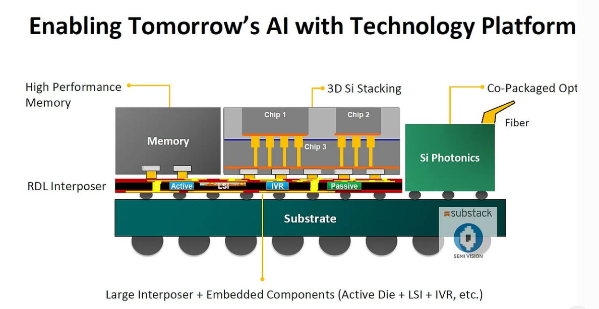
In the short term, MEMS remains mainstream (Google-led), with DLC and DLBS as supplements. In the medium to long term, silicon photonics is expected to dominate due to its speed, cost, and integration advantages, especially when combined with CPO (Co-Packaged Optics) technology to further reduce power consumption. Challenges include standardization (OCP OCS sub-project advancing open specifications), insertion loss optimization, and SDN controller integration (for intelligent traffic engineering).
As AI computing power evolves from "ten-thousand cards" to "hundred-million cards," OCS will form a complementary "optical-electrical hybrid" architecture with electrical switching, ultimately driving a full-optical interconnect revolution. The parallel development of the four technology routes will surely propel the optical communications industry chain into a new wave of explosive growth.
OCS optical circuit switches are reshaping the future of AI data centers at "light speed." Although there are four technology routes, the goal is the same: to allow optical signals to travel freely in the ocean of computing power, paving the optimal path for humanity's intelligent leap forward.


