Basic Manufacturing Process of Laser Chip
2022-11-25
The manufacturing process of a laser chip is similar to that of a semiconductor chip. It must go through a series of processes such as silicon wafer manufacturing, IC design, IC manufacturing, and IC packaging and testing, and finally make into a small chip.
1. Substrate Selection and Preparation
The substrate is used for epitaxial growth and is the first step in device fabrication. Since the result of epitaxial growth is affected by the crystallization quality of the substrate, the substrate must match the lattice of the heterojunction material. It must have an appropriate doping concentration and a certain thickness; the substrate The density of surface and internal defect should be low, and its TTV (Total Thickness Variation), BOW, Ra, etc must be good.
Common geometric parameters: TTV(Total Thickness Variation), BOW, WARP, TIR(Total Indicated Reading), STIR(Site Total Indicated Reading), LTV(Local Thickness Variation)
2. Epitaxial Growth
Epitaxial growth is defined as the condensation of gas precursors to form a film on a substrate. Liquid precursors are also used, although the vapor phase from molecular beams is more in use. Vapor precursors are obtained by CVD and laser ablation. Epitaxial growth is the process of depositing a thin layer (0.5 to 20 microns) of single crystal material over a single crystal substrate usually through chemical vapor deposition (CVD). It is the core process in the manufacture of semiconductor lasers. It is also a key step in determining device performance and yield. It mainly refers to the growth of a single-crystal multi-layer two-dimensional layered structure with precisely controlled component thickness doping on the surface of the semiconductor substrate material to form a homojunction or heterojunction. The material composition, structure thickness and defect concentration control directly determine the wavelength, efficiency and reliability performance of the laser diode chip.
Production Porcess of Epitaxial Growth: LPE(Liquid Phase Epitaxy), MOCVD(Metalorganic Chemical Vapor Deposition), MBE(Molecular Beam Epitaxy), etc.
3. Corrosion & Etching
Corrosion is based on laser design and materials to prepare various structures and shapes required (selective removal of unwanted materials from the surface of silicon wafers). It is divided into wet etching and dry etching.
4. Doping
A certain amount and a certain type of impurities are doped into the crystal can make the amount and distribution of doped impurities to meet the requirements. Doping will change the electrical properties of wafer. Due to the poor electrical conductivity of intrinsic silicon, it can only function as a semiconductor when an appropriate amount of impurities are added to silicon to change its structure and electrical properties. Silicon doping is the basis for preparing P-N junctions in semiconductor devices, which refers to doping the required impurity atoms into specific semiconductor regions to locally dope the substrate and change the electrical properties of the semiconductor.
5. Electrode
Electrode production is also called ohmic contact. The quality of the electrodes directly affects the power conversion and reliability of the laser. Both electron beam evaporation and magnetron sputtering can be used for electrode fabrication.
6. Cleavage & Coating
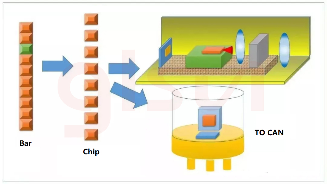
The cleavage technology is to split the wafer into Bars to get parallel reflective cavity surfaces, one side is coated with anti-reflection coating and the other side is coated with anti-reflection coating. Cleavage can also split the bar into single chips, and the chips can be separated one by one via crystal expansion.
7. Mounted
SMT is to paste the laser chip on the heat sink with solder. Gold-tin alloy is generally used as solder. The advantages of gold-tin alloy are high solder joints, high strength, no need flux, and high reliability connection in a small area. Solder has strong thermal conductivity, which is conducive to the heat dissipation of laser. It is necessary to keep the bond firm and the stickiness should be uniform when patching, but the solder used should not be too much, and the temperature should not be too high, so as to prevent the cleavage surface from damaging.
8. Gold Wire Bonding
Bonding is to bond the gold wire to the die to be connected by ultrasonic hot pressing as a lead for current injection. Gold wire generally chooses a gold wire with a diameter of 1 mil (25um) and a purity of 99.999%, and silicon aluminum wire is also used. There are two welding modes: ball bonding and wedge bonding. Wedge welding is used for high frequency, radio frequency and other special applications to avoid signal damage. The photoelectric industry mostly uses ball welding because it is firm and stable.
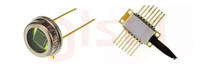
9. Package
In order to improve reliability, the package is fully metallized and sealed to prevent air leakage. General packaging forms include TO-CAN, Butterfly, Gold BOX, etc.